

How can we guarantee the quality of printed circuit board(PCB) we manufactured? Basically we use following treasures and processes to ensure that we always deliver high quality circuit board products to our customers.
1. Design Rules Check(DRC)
The DRC is a quite important step and in-depth review of your production data in PCB manufacturing, which is carried out by our experienced CAM engineers with GENESIS software before production of your printed circuit board. A comprehensive Design Rule Check helps to identify many errors in advance, thus avoiding problems and complaints. We also do the PCB manufacturing rule check to make sure the PCB design is manufacturable. If we find any errors we will get in contact with the customer.
2. Electrical Testing
The electrical testing(E-Test) for circuit boards is performed after manufacture. We use flying probe test for small volume and prototype PCB orders, but use E-Test fixtures to test production batch PCB orders. The tester will check for short circuits, open circuits and make sure the nets of the PCB we manufactured is the same as the nets in your design. PCB boards that are identified as defective are eliminated; defective PCB boards in panels are specially marked.
3. Automated Optical Inspection(AOI)
We use AOI to check the inner layers of multilayer PCB. This inspection is much more reliable and repeatable than manual visual inspection and it will guarantees the high reliability of multilayer circuit boards. AOI visually scans the surface of the PCB. The circuit board is lit by several light sources and observed by a scanner or by a number of high definition cameras. This enables the monitoring of all areas of the printed circuit board. AOI for a bare PCB board inspection will detect the features include:
•Line width violations
•Spacing violations
•Excess copper
•Missing pads
•Cut traces or pads
•Hole breakage.
4. X-Ray
Testing the layer offset with X-ray technology is very important in the manufacture of multilayer PCB. X-ray images are the best (and only) way to identify and correct layer displacements in the pressing process.
Drill holes in multilayer PCB are also optimized using X-ray images. Any minor deviations in the geometry of the circuit board image compared to the geometry of the drill hole coordinates will be identified. By changing a correction factor within a clearly defined tolerance range, it can be ensured that the optimum drill reference point will be determined for each axis, with an optimal interpolation for all layers. These corrections take place in the µm range!
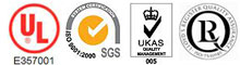
5. ISO9001:2008 and UL certified(UL No: E357001)
We're ISO 9001:2008 certified PCB manufacturer. Our quality control system records the customer requirements and creates a system for communicating with customers about product information, inquiries, contracts, orders, feedback and complaints. Moreover, our quality control system is regularly audited and evaluated for conformance and effectiveness.
All our electronic board products comply with UL safety certification 94V-0. Our UL number is E357001. All our PCBs meet a flame rating 94V-0 and satisfy all UL requirements.
The other Reliability Testings before shipment as below,
1. Plating thickness testing
2. Thermal stress testing
3. Surface peelable testing
4. Impedance testing
5. 100% Visual inspection
6. Solderability testing
7. Ionic contamination testing
8. Metallographic microscopic analysis