

Compare to standard Rigid PCB, HDI PCB request much higher wiring density with finer trace and spacing, smaller vias and higher connection pad density. Blind and buried vias'design is one of their marked feature.HDI PCB are widely used for Cell Phone, tablet computer, digital camera, GPS, LCD module and other different area. The advantages of HDI PCB include:
- Reduce the cost
- Better reliability
- Increase the wiring density
- Increase design efficiency
- Can improve the thermal properties
- In favor of the use of advanced packaging technology
- Has better electrical performance and signal correctness
- Can improve the radio frequency interference, electromagnetic interference and electrostatic discharge
Currently the advanced HDI technology we used include: "Copper Filled" for special stack microvia, "Laser Direct Imaging"(LDI) is specifically designed for fine line technology, to eliminate dimensional stability problem of artwork caused by environmental and material issues. "Direct Laser Drill"(DLD) is drilling of copper layer by direct CO2 laser irradiation, compare to additional laser drilling with conformal mask, the copper direct laser drilling is capable of providing higher accuracy, better hole quality and better efficiency for HDI projects
General Specification for HDI PCB
Layer Count: 4-20Layers
Type of stack up: 1+N+1, 2+N+2
Material Available: FR4, High Tg FR4, Halogen Free FR4
Board thickness: 0.4-3.2mm
Finished copper thickness: 1/3oz – 3oz
Min trace width/spacing: 3/3mil
Min through hole: 0.2mm
Min blind via: 0.1mm
Surface treatment: Immersion Gold, ENIG + OSP
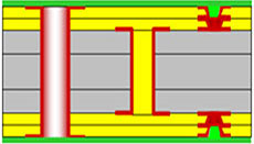
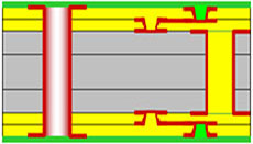
1. High-density interconnection/HDI PCB
Layer: 6(HDI)
Structure: 1+4+1
Material: FR4
Thickness: 0.8mm
Min trace width/spacing: 0.076/0.076mm(3/3mil)
Surface treatment; Immersion Gold
Blind via L1-2 & L5-6: 0.1mm(4mil)
Buried via L2-5: 0.2mm(8mil)
Application: telecommunication
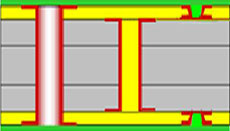
2. High-density interconnection/HDI PCB
Layer: 8(HDI)
Structure: 2+4+2 with stagger via
Material: FR4(Halogen free)
Thickness: 1.0mm
Surface treatment; Immersion Gold
Blind via L1-2 & L2-3 & L6-7 & L7-8: 0.1mm(4mil)
Buried via L3-6: 0.2mm(8mil)
Impedance control: differential 90 & 100ohm
Application: telecommunication
3. High-density interconnection/HDI PCB
Layer: 8(HDI)
Structure: 2+4+2 with stack via
Material: FR4(Tg170)
Thickness: 1.0mm
Surface treatment; Selective Immersion Gold + OSP
Blind via L1-2 & L2-3 & L6-7 & L7-8: 0.1mm(4mil)
Buried via L3-6: 0.2mm(8mil)
Special process: Copper-filled on L2-3 & L6-7
Application: telecommunication