A-TECH Circuits have been specializing in quick turn PCB prototype & small up to middle volume Rigid PCB for decade, our strong process capability ensure that we're able to meet most of your technical requirements and provide the highest quality. Moreover, With our clear market positioning on quick turn PCB manufacturing, our deliveries are guaranteed to be on time.
General Specification for Rigid FR4 PCB
Layer Count: 1-40Layers
Material Available: CEM1, CEM3, FR4, High Tg FR4, Halogen free FR4, Teflon, Taconic, Arlon, Rogers.
Board thickness: 0.2-5.0mm
Finished copper thickness: 1-6oz
Min trace width/spacing: 4/4mil
Min hole size: 0.2mm
Colour of Solder Mask: Green, Blue, White, Black, Yellow, Red.
Colour of Silkscreen: White, Black, Yellow.
Surface treatment: HASL, HAL(Lead free), OSP, Gold Plating, Immersion Gold/Tin/Silver.
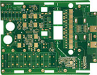 1. Heavy Copper PCB/Power supply PCB
Layer: 4
Material: FR4(Tg170)
Finished copper thickness: 4oz on each layer
Min trace width/spacing: 0.3/0.4mm(12/16mil)
Application: Power controls, Heat Dissipation.
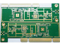 2. Gold Finger & Impedance Computer circuit board
Layer: 6
Thickness: 2.0mm
Surface treatment: ENIG + Hard gold plated on gold finger(Au: 30u")
Impedance control: Single-ended 50ohm, Differential 90ohm
Application: Computer
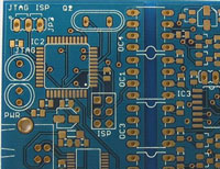 3. Multilayer PCB with Thick gold plating
Layer: 8
Material: FR4(Tg180)
Min trace width/spacing: 0.3/0.3mm(12/12mil)
Surface treatment: Hard gold plating (Au: 50u")
Application: Military
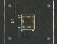 4. Via in pad(VIP) electronic circuit board
Layer: 10
Material; Halogen free FR4
Thickness; 1.6mm
Solder Mask: Matt Black
Special technology: Via in pad, resin-plugged hole on BGA area.
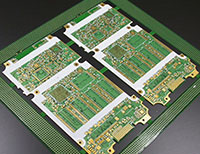 5. Multilayer PCB with Mechanical blind via
Layer: 6
Thickness: 2.4mm
Min through hole: 0.3mm
Min trace width/spacing: 4/4mil
Mechanical blind via L1-3 & L4-6: 0.2mm(8mil)
Application: Telecommunication
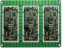 6. Electronic board with gold plating on edge
Layer: 12
Material: FR4
Board thickness: 2.0mm
Surface treatment: Gold Plating
Min through hole: 0.3mm
Special technology: Gold plating on edge


