Our advantages
We have realized the increasingly fierce competition in the field of PCB, in order to remain our competitive on fast pcb, cheap pcb, advanced pcb and continue to win the market, We always pay attention to do continuous improvement and strengthen self construction. The following are a few of our strengths:
1. We could provide PCB industry's fastest pcb turn on PCB prototype and guarantee on time delivery.
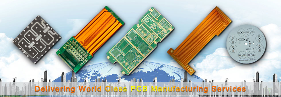
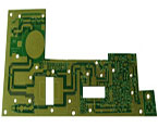
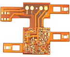
2. We can fulfill most of your PCB requirements and supply a wide range of PCB board, including rigid FR4 multilayer pcb, flexible pcb, rigid-flex pcb, metal core pcb, Microwave/RF pcb and HDI pcb, so you don't need to find new pcb manufacturer if you need some unusual PCBs.
3. We maintain a large inventory of stock PCB material to quickly service a wide range of PCB applications.
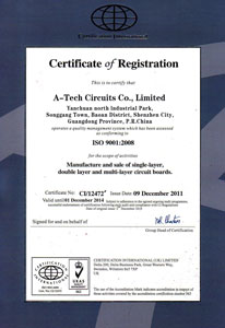
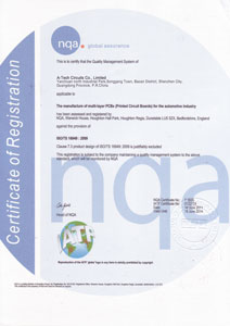
4. Our products and services are 100% guaranteed to be in accordance with IPC-6012 & IPC-A600F standards, and we're certified to IS09001-2008 and UL approval.
5. We provide free engineering review and support. You will be noticed if we find that your PCB design violates our technical requirements or has errors.
6. We're a full service PCB manufacturer, including low to medium volume PCB assembly capability.
7. Extremely fast response time to your needs with quick PCB quote within two hours and rapid service response time.
8. No MOQ requirements, even one piece of PCB board is acceptable.
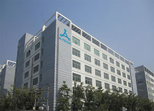
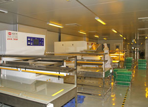
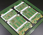
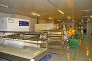
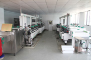
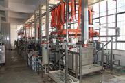
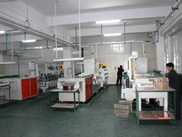
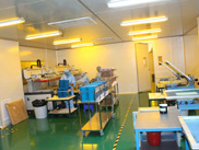
Facility Tour
As a professional PCB manufacturer, we continue to invest in state-of-the-art automation equipments and keeping abreast of the new PCB manufacturing process and technology, our PCB manufacturing process is able to provide very low cost and extremely high yield rated output..
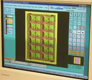 1. Engineering & Artwork generation
The first step in the PCB manufacturing porcess of a new printed circuit board product is the CAM engineer stage. A-TECH uses the most advanced software available today on the market, GENESIS 2000. This tool permits a detailed "Design Rule Check" which can often catch problems before they are manufactured. The next stage is the generation of production PCB artwork.
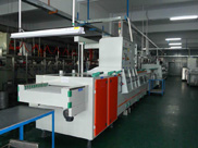
2. Develop-Etch-Strip (DES)Line
After exposure of artwork, multilayer PCB inner cores feed from clean rooms into an integrated system that develops, etches, and strips the inner layers. Inner layer process is to etch and form inner layer circuitry of PCBs. This IS system is stainless steel and titanium. Computers control the parameters of the process, yielding consistent quality. Exiting the line is a finished core.
 3. Automated Optical Inspection(AOI)
Automated Optical Inspection (AOI) equipment is used to inspect all inner PCB layers before proceeding to the next step in PCB manufacturing. This process identifies opens, shorts, and reduced traces after pcb etching. It is better to locate these problems early in the process, prior to lamination.
 4. Lamination
This equipment is used to press PCB inner cores, prepregs and copper foils together to be multilayer PCB panels. It features hot oil heated beds with vacuum for outgassing. Load systems move the panels from the hot presses to the cold press/cool down stages of the process. The entire lamination process is computer controlled.
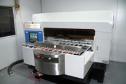
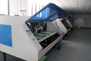 5. CNC Drilling machines
Drilling is very critical to the PCB manufacturing process, we use Hitachi six spindle machines for medium to high volume PCB manufacturing, For small lots, we utilize two spindles machine but drill the same panel stack. They feature auto-load and unload for lights off operation. These are excellent for prototype PCB manufacturing due to their quick setup and unsurpassed speeds.
 6. Automatic Dry Flim laminator
The panels continue directly into the Clean Room passing through the auto-laminator receiving dry film Photo-resist for the outer layer imaging process. Again this type of automation reduces time and increases the quality and overall efficiency of the process.
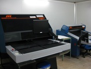
 7. Imaging Exposure machine
Imaging is performed in clean rooms utilizing Colight 1630 7Kw exposure units that are outfitted with C.A. Picard registration systems featuring vacuum hold-down, which creates excellent artwork registration. Rooms are temperature and humidity controlled. This photo process places an image of the circuit onto the drilled panel.
 8. Developing machine
Exposed panels exit our clean rooms feeding directly into IS developers that develop the photo resist. Panels are then moved to copper/tin plating.
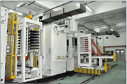
9. Automated Plating line
 Copper/tin plating is eductor-based, allowing high aspect-ratio plating with superior copper distribution characteristics and surface to hole ratios. High output rates coupled with low labor content is an added plus. Based on the photo image film of the desired circuit, copper, then tin, is plated on the circuit image.
10. PCB Etching machine
 After plating, the process panels travel to the pcb etching process. pcb etching Process is one of the major steps in the chemical processing of subtractive printed circuit board. It is the removal of copper, to achieve the desired circuit patterns. PLC and in-process sensors provide excellent real-time control of the process. All copper is removed except the circuitry that is protected by the tin plating applied during the previous process. The tin is then stripped and the copper is cleaned and the newly prepared circuit is ready for solder mask.
 11. LPI Solder Mask
Liquid Photo-Imageable (LPI) solder-mask is applied and processed utilizing automated Argus horizontal spray or DP1500 vertical systems. A-TECH can process many types and colors of masks in pcb manufacturing. Once the panel is exposed and developed, it moves through final cure and on to final surface coating.
 12. Automatic V-cut machine
State-of-the-art Accuscore scoring equipment is used for fast, accurate V-grooving. X and Y tolerances are held to ±0.004". CNC routing is also utilized to remove individual parts or arrays from the process panel.
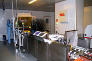
13. Electrical test machine
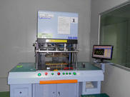 Electrical test machine is used to detect opens or shorts in pcb etching if they exist before PCB shipment, It is insurance for the customer, that he will receive functional circuit board products and avoid the costly assembly of defect PCB products. Normally we used flying probe test machine for PCB prototypes and small quantity orders, but used E-Test fixture for large quantity/batch PCB orders which is more efficient.